This describes the clock synchronization in the GMPS/GEPS in BM/TC combined configuration mode.
Clock Synchronization in the GMPS/GEPS (BITS Clock Source)
Figure 1 shows the clock synchronization in the GMPS/GEPS that uses the BITS clock source.

The clock signals in the GMPS/GEPS are processed in the following manner:
- The BITS clock signals are transmitted to the GGCU through the GGCU panel.
- After a phase lock in the GGCU, the BITS clock signals change into 8 kHz clock signals.
- In the GMPS, the 8 kHz clock signals are transmitted from the GGCU to the GSCU through the backplane.
- The 8 kHz clock signals are transmitted from the GGCU panel in the GMPS to the GSCU in the GEPS through a Y-shaped clock cable.
- The GSCU in the GMPS/GEPS transmits the 8 kHz clock signals to the other boards in the GMPS/GEPS through the backplane.
Clock Synchronization in the GMPS/GEPS (Line Clock Source)
Figure 2 shows the clock synchronization in the GMPS/GEPS that uses the line clock source.
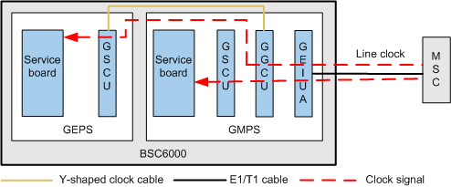
The clock signals in the GMPS/GEPS are processed in the following manner:
- The GMPS extracts line clock signals over the A interface. The line clock signals are processed by the GEIUA/GOIUA and then are converted into 8 kHz clock signals.
- In the GMPS, the 8 kHz clock signals are transmitted to the GGCU through the backplane. After a phase lock in the GGCU, the 8 kHz clock signals are transmitted to the other boards in the GMPS through the GSCU.
- The 8 kHz clock signals are transmitted from the GGCU in the GMPS to the GSCU in each GEPS. Then, the GSCU in each GEPS forwards the clock signals to the other boards in the GEPS.