Appendix A. Plug and Play Standard Registers
The figure below illustrates the order of the card registers and the logical device registers. As this figures shows, the card registers are unique for each card. However, the logical devices registers are repeated for each logical device on the card. Table A-1 contains the descriptions for the card-level registers and table A-2 contains the descriptions for the logical device registers. NOTE: Any unimplemented registers in the range 0x00 to 0x2Fh must return 0 on reads.
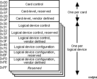 Figure A-1. Plug and Play Register Map