Jeff Epstein, Future Domain Corporation
Steve Timm, Microsoft Corporation
July 29, 1994
The SCSI interface is known for its breadth of device support, range of performance options, and external peripheral expansion. Yet it's difficult for most PC users to configure add-on SCSI devices. Board level jumpers, switches, and setup utilities are commonly used in the configuration sequence. It's no wonder that SCSI has become a target for Plug and Play (PnP) design, enabling end users to quickly and easily change their peripheral configuration to meet personal computing needs. For SCSI product vendors, PnP offers consistent design parameters, enhanced device interoperability, and lower support costs.
Within the PC architecture, supporting PnP developments (including a PnP BIOS and a PnP operating system) will enable jumperless design of add-in SCSI cards. When PnP devices are used with a Plug and Play operating system, devices are automatically configured. For example, system resources such as IRQs, address spaces, and DMA channels are uniquely and automatically assigned to PnP ISA cards by the BIOS during the boot cycle and dynamically by the operating system during run time. But extending PnP to the SCSI bus poses a unique set of design issues.
Following the lead of PnP BIOS and PnP ISA ("Adding PnP Capability to an Existing Card," Electronic Design, February 7), industry leaders Adaptec, Future Domain, Maxtor, Microsoft, and NCR initiated a proposal for PnP SCSI in mid-year 1993. This specification has since been refined through Microsoft's open process design review, and Rev. 1.0 was released to the public in March 1994. The PnP SCSI specification, coupled with ANSI/X3T10's approval of the SCSI-2 ANSI X3.131–1994 specification in February 1994 and the nearing completion of SCSI-3 SPI, signifies the maturity of SCSI technology.
For SCSI, PnP defines optimum design choices in reference to existing SCSI standards. The PnP SCSI profile is targeted for volume PC applications. While SCSI-3 SPI defines supporting component-level requirements, PnP SCSI defines system-level design parameters required for automatic installation and configuration of SCSI devices. PnP SCSI outlines designs for PC SCSI subsystems, host adapters, and peripherals (disk, CD-ROM, and so on). Primary components of PnP SCSI technology include a PnP cable connector, automatic electrical termination of the SCSI bus, and automatic configuration of SCSI IDs during the PC's boot cycle. Additional guidelines contribute to the overall framework.
Electrically, the SCSI bus exhibits the noise characteristics of a transmission line. Assuming an electrically consistent set of cables, connectors, and printed circuit stub lengths per SCSI-3 SPI, a chain of SCSI devices can effectively terminate the bus by activating termination components located at each end of the bus. For PnP, the issue is how to design a digital solution for an analog problem that requires dynamic adjustment whenever the SCSI configuration changes.
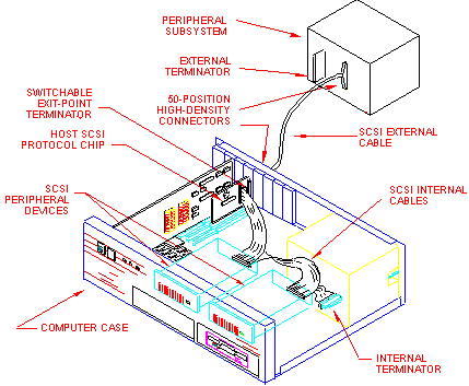
A PnP SCSI chain internal to the PC enclosure must be self-terminating. This allows external expansion without the need to remove the system covers. Self-termination is readily achieved by a standard PnP cable configuration (see Figure 1) with an active termination component at the internal cable end, and a second exit point terminator located on the host adapter. PnP eliminates the cost and complexity of each peripheral having to provide bus termination. Instead, individual termination components are replaced by a system design for bus termination.
Figure 1. Mixed (internal/external) SCSI configuration
Internal SCSI buses that are routed to an external SCSI connector require some form of automatic termination. The exit point terminator, located conceptually at the mid-point joining the internal and external SCSI buses, must be enabled whenever an internal-only or external-only SCSI chain is attached to the host adapter. For a mixed SCSI configuration, the exit point terminator must be disabled when a peripheral device is attached to the external SCSI connector. This allows the internal bus to be extended outside the PC enclosure. In this scenario (see Figure 1), an external terminator is plugged into the only open connector on the external chain of SCSI devices. The automatic termination component must be located close to the exit point connector to avoid excessive stub lengths from affecting signal quality. In some cases, this terminator may need to be integral with the exit point connector assembly.
One approach to PnP termination used by Adaptec senses the current flow on the reset line to determine whether the lines are properly terminated. The termination circuit connects directly to both connectors, and a third contact is separated from each connector by a 5-ohm resistor for current sensing. During the reset cycle, the termination circuit senses the current sink to each connector. If the current from either connector is less than 10mA after 1 microsecond, the termination component activates to pull up the line. Termination components supporting this technique are in development by Dallas Semiconductor (part no. DS2109).
Another approach to automatic termination is to detect the attachment of a SCSI device on the external connector. If no SCSI device is attached to the external PC enclosure, the host adapter is located at one end point of the internal SCSI chain, and the automatic termination circuit must be enabled. Connectors exist to support this technique by activating a ground signal when an external cable is attached. While effective, this mechanical solution suffers the fate of introducing yet another connector with low-volume pricing.
The circuit consists of a pull-up resistor attached to a single ground line on each of the adapter's SCSI connectors. Pin 22 is used on the internal connector, while pin 34 is used on the external connector. These two signals drive the control logic on the host adapter's termination circuit. The switchable active termination component is disabled whenever both input signals are low, indicating the presence of a device on the internal and external SCSI chains. If either input signal is high, the terminator is enabled to terminate one end of the internal or external bus.
This circuit is an excellent choice for PnP SCSI host adapters and is effective for multi-initiator systems as long as the adapters are separated by at least one SCSI peripheral. While satisfying requirements for PnP SCSI adapters, additional design will be required to extend this termination concept to all SCSI peripherals since it relies on adjacent devices to maintain the SCSI ground signals. Another possible constraint in the design of self-terminating peripherals is bus loading. For "fast SCSI" timing, multiple disabled automatic termination components could affect timing margins. Table 1 lists availability of switchable termination components.
Table 1. SCSI Termination Components
| Manufacturer | Part No | SCSI Lines | DC Output current | Output Capacitance |
| Unitrode | UC5602 | 18 | 17.1>22.4 ma | 11 pf |
| Unitrode | UC5604 | 9 | 17.1>22.4 ma | 10 pf |
| Unitrode | UC5613 | 9 | 19.1>22.4 ma | 3 pf |
| TI | TL2218-285 | 9 | 19.0>22.4 ma | 8 pf |
| Motorola | MCC142236 | 18 | 19.5>23.0 ma | 7 pf |
| Motorola | MCC142237 | 9 | 19.5>23.0 ma | 7 pf |
| Dallas Semi | DS2107S | 9 | 21.3>23.2 ma | 8 pf |
| Micro Linear | ML6509 | 9 | 24 ma max | 6 pf |
| Rohm | BH9590FP | 18 | 15>30 ma | — |
All SCSI devices require a unique SCSI ID that is set today by a switch on older legacy devices. Conflicts occur when two or more devices have the same ID, resulting in failure of the controller to recognize one or both devices. This condition forces end users to review switch settings for the entire SCSI chain or to randomly change ID switches until the system works. To solve this problem, several ANSI SCSI committee members led by Quantum and Digital Equipment Corp. defined a new protocol known as "SCAM" (SCSI configured automagically). SCAM allows PnP peripherals to have their SCSI ID automatically assigned by a PnP host adapter. In the fall of 1993, the SCAM protocol was formally approved by the ANSI committee for addition to the draft ANSI SCSI-3 Parallel interface (SPI) document.
Devices supporting the SCAM protocol are fully backward-compatible with the installed base of "legacy" SCSI peripherals. Legacy devices retain their default IDs based upon jumper settings, since these IDs are not programmable. In the reverse scenario, PnP SCAM peripherals connected to a legacy host adapter respond to their default (jumpered) ID the same way legacy devices do today.
While SCAM defines two levels of functionality, PnP SCSI requires Level 1 only. Level 2 incorporates provisions for multi-initiator support and response to ID assignment requests from late-arriving ("hot plugged") SCSI peripherals.
Generally, only firmware changes are necessary to implement the SCAM protocol. However, there are a number of hardware design considerations. First, the SCSI interface silicon must be capable of driving the state and timing of data and control signals under program control. While many chips do this, some will require redesign to support SCAM. Second, Plug and Play will likely require an additional 2K of ROM space to implement the protocol. Third, SCSI ID switches will need to remain accessible on the peripheral device to allow for backward compatibility with the installed base. Additional SCAM hardware design considerations are summarized in Table 2.
Table 2. SCAM Level 1 Hardware Checklist
| Item | HBA | Peripheral |
| 1. Default ID = 7 | x | |
| 2. Configurable ID (overrides default ID) | x | |
| 3. Discrete control over all bus signals | x | x |
| 4. Arbitrate with initiator ID = 7 | x | |
| 5. Respond to selection with a null target ID | x | |
| 6. Delay responses to default ID by 4 ms. | x | |
| 7. Assert BSY after SEL within 1 ms. | x | |
| 8. Detect BSY after SEL within 1 ms. | x | |
| 9. Can respond to SEL within 250 ms. after reset | x | |
| 10. Can respond to SEL within 5 seconds after power-up | x | |
| 11. Can accommodate new BSY/SEL/MSG states | x | x |
| 12. Can disable active negation on DB<7:0> | x |
The timing characteristics outlined in Table 2 are generally not difficult for the designer to incorporate within the firmware of the host controller or peripheral device. A particular interesting characteristic is item 6. A peripheral normally responds to its ID selection as soon as possible. For SCAM, the PnP peripheral must wait for a 4-millisecond period to elapse before responding. This delay is used by the host adapter to distinguish PnP peripherals from legacy peripherals with nonprogrammable IDs.
SCAM requires several "states" to perform the bus protocol as shown in Figures 2 and 3 below. Because the SCAM protocol defines new BSY/SEL/MSG states on the bus, some debug analysis test equipment will be unable to detect the new states. To aid the designer, SCAM Protocol Analyzers are available from Ancot Corp., Menlo Park, California.
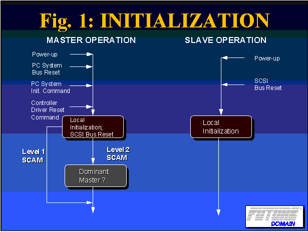
Figure 2. SCAM initialization sequence
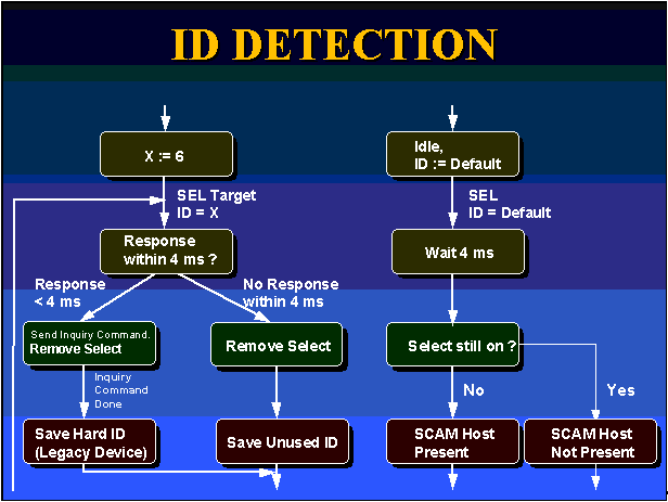
Figure 3. SCAM ID detection and assignment
Figure 3 shows that the host controller first determines whether it is to be the "dominant master". This operation is optional for SCAM level 1 controllers, since multiple host controllers are not present in this configuration.
The host adapter next queries or scans the bus looking for non-SCAM peripherals. The host performs a normal arbitration/select sequence for each ID value, ranging from 6 through 0. SCAM peripherals will automatically delay 4 ms. before responding to their default ID selection. Non-SCAM peripherals will respond immediately in less than 4 ms. This timing difference gives the host the ability to differentiate between a mixed configuration of legacy and PnP peripherals.
The host adapter must save the ID values found to be already in use by the non-SCAM peripherals. These represent the IDs that may not be assigned to SCAM peripherals.
Next, the host adapter performs the SCAM isolation and ID assignment protocol. The data bus bits, 0 to 7, are used during isolation for multiple bus transfer cycle handshakes. Figure 4 shows the information communicated between the host controller and the peripheral.
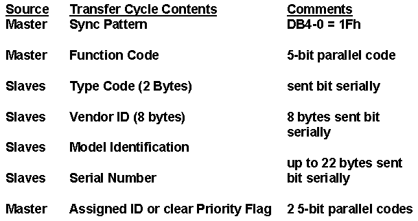
Figure 4. SCAM transfer cycle data
The handshake timing uses DB<0:4> for "data" and DB<5:7>. For each field transfer, the most significant byte and most significant bit are sent first. During the isolation process, a SCAM target uses its standard SCSI inquiry identifier string to differentiate itself from all other SCAM targets on the bus. It does this by performing each data transfer cycle transmission in a bit serial fashion using only two lines: DB0 and DB1. The host controller, however, uses all five DB lines for its transfers.
The target bit serial coding is shown in Table 3. The entire process may be considered an arithmetic comparison done bit-serially. For the first serial transfer, each target checks the first bit of its own inquiry string. If the first bit is a "1", the target drives the DB1 line; otherwise, it drives the DB0 line. If one or more of the targets has a "1", the process proceeds to the second bit. If all of the targets have a "0" for the first bit, the process proceeds to the second bit as well. If the DB1 line is driven by one target, but other targets have a "0" inquiry string bit, that target may be considered to have a lower arithmetic string. The target drops out of the isolation process because it "lost."
Table 3. Isolation Bit Serial Codes
| Target's Inquiry Bit | DB1 | DB0 |
| 1 | driven | — |
| 0 | — | driven |
| none | — | — |
The bit serial compare process repeats until each target runs out of inquiry string bits. When it has no more bits, it ceases to drive either the DB0 or DB1 line. When all targets run out of bits, the host knows that one of the targets had the largest arithmetic inquiry string value. It has isolated one target from the rest of the targets.
The ID assignment process follows the isolation process. The host sends an ID to the winning target using the DB<0:4> lines. The host then repeats the full isolation process for all remaining SCAM targets that have not had their ID assigned yet. When all targets have their IDs assigned, there should be no duplicates or conflicts.
Another PnP design alternative stems from PnP SCSI's requirement for host adapters to consistently assign SCSI IDs to maintain a consistent boot device and drive letters. This can be accomplished using the SCAM ID assignment algorithm called out in the PnP SCSI spec (section 8.2) or optionally through the use of NVRAM on the host adapter. NVRAM in this application is used to track SCSI IDs and drive number (80H, 81H, and so on) assignments per a unique device ID string derived from SCSI inquiry data.
While NVRAM is not required for PnP SCSI, it can eliminate drive letter changes resulting from the addition of a peripheral device to the SCSI chain. NVRAM can also be used to maintain the boot device following addition of a second boot drive to the system. In the short term, system designers should select a motherboard PnP BIOS manufacturer that allows ATA/IDE drives to co-exist with SCSI drives. Then the user can select either one for boot purposes without disabling the other. In the longer term, PnP will require a platform-independent system architecture to select the boot channel (for example, IDE, SCSI, PCMCIA) and boot device.
PnP SCSI peripherals eliminate the need for users to set switches or to disassemble the unit when reconfiguring the system. Hardware requirements include designing in a self-resetting circuit for "term power," removing internal termination components, and exposing two 50-position, high-density connectors on the external peripheral enclosure. Polyfuse devices, such as RBE130 by Raychem in Santa Clara, work well for printed circuit applications. Removing termination components from the internal device can reduce cost, but in the short term, peripherals must maintain their ID switches to ensure compatibility with legacy devices.
A key requirement is the firmware implementation of the SCAM Slave protocol discussed above. The amount of added code will most likely not raise the product's manufacturing cost. Also, existing peripherals that use flash memory for firmware open the possibility for SCAM firmware upgrades. In the software arena, standard command sets for SCSI peripherals are spelled out in the formal ANSI SCSI-2 specification. For PnP, command sets are being refined to enable the interoperation of devices of a given type with a common device driver. Current work is focused on CD-ROM, but additional devices are planned. See Appendix D of the PnP SCSI specification for command references.
SCSI integrated onto the motherboard is the optimum choice for PnP because it eliminates cost and configuration of an add-in host adapter card. This configuration requires integration of the SCSI controller manufacturer's BIOS code into the motherboard's BIOS code. For add-in cards, PnP system components, including a PnP BIOS and a PnP operating system, will greatly simplify ISA adapter installation.
Cabling is another key issue for PnP SCSI systems. Today, five popular SCSI connectors result in up to 15 cable configuration choices. The 50-position, high-density connector was chosen for PnP for its small footprint, lower cost, and increasing volume coupled with the acceptance of "fast 8-bit SCSI." However, PnP SCSI may consider adopting the 68-position, high-density connector for workstations at a later date if a standard icon can be displayed on the connector to aid end-user cable selection. Note that PnP does not specify connectors internal to the PC or internal to the peripheral enclosures.
Another PnP system design parameter is automatic negotiation of the transfer protocol. Host adapters must automatically accommodate the various SCSI bus "synch" protocols. This includes asynchronous, synchronous, and fast synchronous. The recommended PnP solution is for the host adapter to negotiate with the peripheral for the protocol to be used in the data transfers.
When negotiating for SYNC data transfer operation, the host adapter begins by sending a 5-byte SDTR (synchronous data transfer request) to the peripheral. Byte 2 contains the actual sync request code, and byte 3 contains a number representing the transfer period. The smaller the value for byte 4, the faster the transfer period will be. For FAST SYNC operation, a typical value for byte 3 may be around "19h". For slower SYNC operation, a typical value may be 35h. The adapter firmware maintains a table containing the appropriate values for the various devices it supports.
If the peripheral returns a MESSAGE REJECT, the peripheral is notifying the adapter that it does not support that particular speed of SYNC operation. At that point, the controller must keep sending SDTRs with larger numbers until the target accepts the message. If the target ultimately does not accept any of the various large numbers, the controller and target default to ASYNC operation. Most FAST SYNC targets return a multiple byte message that spells out the preferred value for byte 3. In this scenario, the adapter and peripheral directly establish the fastest possible SYNC data transfer operation.
Appendix C of the PnP SCSI specification provides a compliance checklist for peripherals, host adapters, and systems. However, to fulfill the promise of PnP SCSI, additional work is in process to define an industry standard compliance test procedure. Such procedures could be used by device vendors with cross-checks by adapter vendors to ensure interoperability between a matrix of legacy and PnP devices. Beyond individual device testing, certification of PnP devices for a PnP operating-system environment, such as the upcoming release of Microsoft® Windows® 95, will serve to broaden the test matrix and include PnP device drivers for optimum compatibility assurance.
For further information on any of these subjects, see the following forums and bulletin boards:
CompuServe® (GO PLUGPLAY)
SCSI BBS (719-574-0424)